

In Part I of RCRTV’s AI TechTalk interview with Jean-Philippe Fricker, we spoke of exuding confidence when dealing with venture capitalists and deal teams who don’t have the domain experience to understand that a “crazy idea” isn’t so crazy. In Part II, “JP” talks of what “wafer scale” really means, not only in tokens per second (TPS), but in AI inference, thermal management and energy efficiencies.
To start, Fricker describes what he believes is the tokens-per-second (TPS) advantage of Cerebras wafer-scale architecture, which eliminates the off-chip communication bottleneck of traditional GPUs – storing the entire model in on-chip memory and making it one of the fastest, if not the fastest, AI inference solutions in the world for latency-critical, high-performance AI workloads. Recently, Cerebras reached a major performance milestone, running the massive 1T-parameter-open-weight AI model Kimi K2.6 at 981 output tokens per second, making it 6.7 times faster than the next-fastest GPU-based cloud provider (according to Artificial Analysis).
“TPS depends on the workload, but for HPC, we are multiple orders faster, from 3x to sometimes 1000s-of-times faster,” he contends, adding that some researchers have found Cerebras’ WSE to be “faster than even supercomputers in terms of speed and the amount of energy needed for a solution.” For AI and LLMs (especially inference), Fricker says wafer scale can be multiple orders of 10x to 20x faster, though he does acknowledge that for certain HPC workloads, that is not a universal truth, since on-chip SRAM does ultimately hit a “wall” of capacity.
HPC supercomputers in climate modeling or astrophysics, for example, handle terabytes or petabytes of system memory, so there are instances where data does not fit the Cerebras wafer. “If the model has been engineered – designed and architected – for a GPU, fitting really well on the GPU, it might not take advantage of some of the features we have. In other cases, you would allow the underlying mathematics in the LLM to be mapped differently, to take full advantage of the wafer-scale architecture. There are certain models in which that is easier than others.”
Packaging matters: do big things over small distances
When discussing thermal management or power consumption in large data centers, chips are a major culprit in power consumption. In modern data centers, processors are the largest consumers of electricity. How they are physically packaged translates into energy efficiency and limits.
Silicon processors (CPUs, GPUs, and custom accelerators) account for roughly 40% to 70% of a modern data center’s total IT power draw, and every watt of power consumed by a chip turns directly into heat. Of course, data center operators understand all too well that removing that heat requires enormous cooling effort (via fans, pumps, chillers), which can add an extra 30% to 50% overhead to data centers’ energy bills.
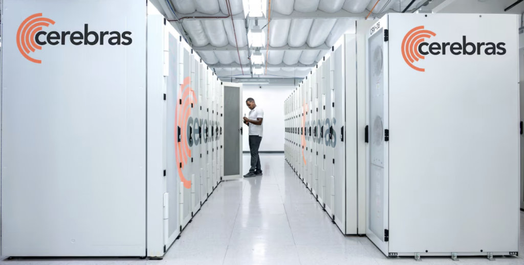
According to Fricker, a single Cerebras system can replace dozens of traditional GPUs, drastically lowering the total energy consumed, despite the 23kW-25 kW of power the Cerebras CS-3 system draws when running a full-load compute task.
“Reducing the power consumption for communicating data from one place to another…moving the data often requires energy, especially at the scale of larger language,” Fricker explains. “It’s a massive amount of data to move.” The Cerebras approach is to do big things over short distances. “We found that by using short connections and very small physical geometries, we reduce the capacitance on those traces, and subsequently, the amount of energy needed to communicate one bit across.”
“We found that by using short connections and very small physical geometries, we reduce the capacitance on those traces, and subsequently, the amount of energy needed to communicate one bit across.”
Jean-Pierre Fricker
Unlike NVIDIA or AMD, which manufacture many small, individual square chips on a circular silicon wafer, Cerebras’ giant, dinner-plate-sized chip is fundamentally more energy-efficient and faster than a cluster of traditional GPUs, according to Fricker, who refers to “short connections,” and “small geometries” as advantages:
- Short Connections (< 1 mm): On a standard multi-GPU setup, data traveling from one chip to another must leave the silicon, pass through packaging substrates, cross a motherboard or circuit board (PCB), and sometimes travel through copper cables. Cerebras keeps it all on a single piece of silicon, with tiny copper wires (“traces”) of less than a millimeter connecting the cores;
- Small Physical Geometries: With Cerebras, the network is completely internal to the silicon wafer rather than being routed across external system components, so the wires can be etched at microscopic, sub-micron scales;
- Reducing Capacitance: Microscopic, millimeter-short internal silicon traces drastically reduce capacitance, with less resistance than would be the case with longer and thicker external system wires;
- Less Energy per bit: Because the capacitance is minimized, it requires less voltage and current to toggle an electrical signal between a 0 and a 1.
“Wafer scale invites ‘small features’ or ‘proximity’ that eliminate the need for a high-energy amplifier to transmit something through a wire that has to span a few inches on the board, or maybe a meter to go to the next rack, or maybe an aisle or multiple aisles,” explains Fricker.
Wide and slow vs. narrow and fast
By making a fundamental design choice to use “wide and slow” electronic interconnects rather than optical or high-frequency links, Cerebras aims to slash wire speeds and reduce energy consumption. Lost speed is recovered by adding “free” wires in parallel on the giant wafer. “You can stay in electrons, rather than transform into light, while also improving the efficiency of communication by slowing the speed at which you communicate on a given wire. You put as many wires as you can in parallel,” says Fricker, who posits that the number of wires on the wafers are essentially free. “That’s different than when you go off chip and don’t have a lot of space, or a lot of perimeter on the chip to get in and out.”
Going faster on one wire, in and out of the chip, requires more energy. “To go from one system to another means you cannot have many wires between the systems. Then you need the fiber optic cable to go even faster. And every time you go faster and faster on a given wire – on a given data transmission channel – you have to expend energy.”
Cores as the ‘secret sauce’
On the Cerebras WSE are “cores,” which are microscopic, independent, fully programmable data flow processors. Each individual core of the 900,000 cores on a single piece of silicon. “That means you get dynamic configuration as needed,” says Fricker, noting that having many wires on a wafer offers nearly endless workarounds: “If one core can communicate with four adjacent ones, you can add more wires to maybe go further than just the adjacent one. You pick the wire that works and don’t use the wire that doesn’t work. In other words, you work around a faulty element.”
Because each individual core is incredibly small, measuring roughly 0.05 mm², there is an incredible tolerance to defects. A speck of dust that ruins a few cores during manufacturing is not catastrophic, since software can deactivate broken cores and routes the mesh fabric around them.
“There is no such thing as a perfect wafer. We have to deal with defects. The more tolerant to defects we are, the more we can use the not-so-good materials,” explains Fricker. “You still have minimum criteria for exposing this to your customer…too your workload, so you create an architecture that allows you to maintain that minimum, while forgiving a lot of defects.”
This tolerance to defects is especially meaningful now, when supply chain constraints and competition for fab access is fierce. “There are multiple components in the system, each of which might have supply challenges. With silicon, fabs in the world are in limited qualities, with everyone competing for access to the throughput of a fab, so it’s very important to get as high a yield as you can from your supply.” For Cerebras, the wafer-scale design means more can be drawn from manufacturing yields. “By having an architecture that’s more fault tolerant, by using smaller cores closely connected to one another, we’re able to be more immune to the shortage of wafers.”
What’s to come: agentic and inference
Fricker believes wafer-scale technology is uniquely positioned for the Agentic AI era because agentic workflows transform inference from a single “chat” into multi-step execution loops. “With more talk of inference and agentic AI, it’s very exciting to think of what our technology will enable in different sectors.”
He says that so many of the domains he thought would “take a long time” to use AI are now embracing it at unprecedented speeds. “Every day, there’s compounding improvement,” says Fricker. “What excites me is to see that there is a completely new generation of thinkers out there that will use these tools in creative ways, beyond what the originators of the tools thought was possible. People are starting to use our systems in ways that we did not anticipate…empowering and amplifying what people can do, in scope, in breadth, in speed.”