

Table of Contents
Cerebras packs three WSE-3 Turbo wafers into one rack
In sum – what we know:
- Three wafers per rack – The CS-4 Nexus architecture houses three WSE-3 Turbo engines, lifting sparse FP16 compute to 750 PFLOPS per rack from 125 in the CS-3.
- Same silicon, more power – The WSE-3 Turbo keeps the CS-3’s 900,000 cores and 44GB of SRAM, with gains coming from packaging, power delivery, and higher clocks.
- Stacked DRAM roadmap – The CS-6 will stack DRAM above the wafer’s logic and SRAM to ease a capacity problem stuck since 2021, while the CS-5 lands in 2027 on new silicon.
Cerebras has begun rolling out its CS-4 wafer-scale AI system in a fundamentally different package than anything the company has shipped before. The new Nexus rack architecture houses three wafer-scale engines instead of one, rethinking the rack itself around compute, power, and I/O rather than traditional server form factors. Alongside the CS-4, the company also previewed the CS-6 — a future wafer-scale engine that will stack DRAM directly on top of the wafer’s logic and SRAM layers.
On one hand, there’s a practical, near-term hardware release that squeezes considerably more performance out of existing silicon through aggressive rack-level engineering. However, there’s an ambitious roadmap bet designed to solve the memory-capacity problem that has quietly followed Cerebras through several generations of hardware.
CS-4 hardware and the Nexus rack architecture
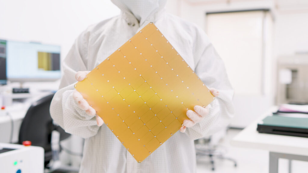
The CS-4 is built around the WSE-3 Turbo, an overclocked version of the existing wafer-scale engine fabricated on the same 5nm TSMC process as the WSE-3 in the CS-3. It retains the exact same 900,000 AI-optimized cores and 44GB of on-wafer SRAM as its predecessor. In other words, the gains come from packaging, power, and clocks rather than new transistor designs.
On-wafer SRAM capacity rose from 40GB in the WSE-2 (2021) to 44GB in the WSE-3, and has been stuck at 44GB since — a stagnation that puts increasing pressure on the hardware as models continue to expand. It’s the most obvious limitation the CS-4 doesn’t address, and it explains why the CS-6 preview exists at all.
Where the CS-4 does move the needle is the Nexus rack itself. A single Nexus rack houses three WSE-3 Turbo wafers, tripling per-rack compute density compared to the single-wafer chassis used in the CS-1 through CS-3 systems. The design splits the rack into a front half dedicated to shared power equipment and a rear half of modular compute “backpacks” — self-contained assemblies that integrate the wafer, power conversion, liquid cooling, and I/O. Technicians can install or swap a backpack from the rear without disturbing the front-mounted power gear, which should meaningfully reduce service complexity. Cerebras also claims the standardized modules enable about 60% more manufacturing automation than earlier systems.
Power conversion has been moved to within roughly 0.5 millimeters of the wafer — about 100x closer than conventional GPU-board power delivery — enabling more efficient, higher-current delivery. Combined with direct-liquid cooling on each wafer module, that supports a per-wafer power budget roughly double that of earlier systems. That’s what earns the “Turbo” designation.
Performance and bandwidth scaling
The headline number is 750 PFLOPS of FP16-class AI compute per rack — a sparse figure, per Cerebras’ own footnote, with third-party estimates putting the dense FP16 equivalent at roughly 75 PFLOPS. Worth noting that most of that comes from tripling the wafer count and doubling per-wafer power, not from any single breakthrough. Cerebras also says the system supports models with more than 50 trillion parameters.
The data-movement numbers scale in step. Rack-level memory bandwidth jumps to 129.6 PB/s, up from 21.6 PB/s in the CS-3, while internal fabric bandwidth grows to 160.5 PB/s from 26.7 PB/s. System I/O rises from 1.2 Tb/s to 7.2 Tb/s. The CS-3’s roughly 5-microsecond figure is off-wafer I/O latency — a single-wafer system has no wafer-to-wafer path — while the CS-4’s as-low-as 2 microseconds is wafer-to-wafer latency over the new Direct Wafer Links between backpacks. Networking supports standard RoCE v2 alongside Cerebras’ proprietary Direct Wafer Links, so the rack isn’t locked into a fully proprietary fabric.
Cerebras itself headlines up to 30x faster than GPU-based solutions, though that’s a best-case, single-stream figure — tokens per second per user on one model (GPT-OSS-120B at 4,465 tok/s versus 131 on an unnamed GPU deployment in Cerebras’ own demo), not a blended hardware metric. That said, rack-level engineering can deliver a generation’s worth of performance without a new silicon node — much the way Nvidia has extracted gains from denser pod packaging and better boards around existing GPU dies.
The CS-6 preview and stacked DRAM
The CS-6, positioned “two generations out,” is where Cerebras plans to finally attack the memory-capacity problem head-on. The design integrates 3D-stacked DRAM directly above the wafer’s logic and SRAM layers, connected through ultra-high-bandwidth vertical interconnects. The goal is to keep a much larger fraction of model parameters resident right next to the compute cores, rather than relying on off-chip DRAM pools and networked scaling. That preserves the short-distance data paths that give Cerebras its inference advantage over GPU systems, which pair HBM with individual dies connected over large meshes. Cerebras claims the result will be an “order of magnitude smaller footprint” for frontier-scale inference compared to traditional multi-GPU clusters — a claim that will need real hardware behind it before it means much.
A transitional CS-5 system got a briefer mention: targeted for 2027, it pairs the Nexus platform with a next-generation wafer-scale engine — new silicon, not just rack and software scaling. Cerebras is aiming for up to 10,000 tokens per second per user on leading open-source models like Gemma 4 31B and gpt-oss-120b, with up to 5,000 tokens per second per user and 3 million tokens per second per megawatt on the largest frontier models. It reads as a bridge product, keeping the Nexus trajectory going while the harder CS-6 work matures.
And that work is genuinely hard. Stacking DRAM over a full wafer introduces thermal and power-density challenges well beyond conventional HBM-on-die integration — vertical stacking adds heat sources directly above the compute layer, across an area vastly larger than any GPU die. Yield is the other big risk. Stacking increases the odds that defects in either the logic or DRAM layers compromise usable area, and Cerebras hasn’t said how it plans to partition or route around bad regions.
There’s a lot we don’t know. Total DRAM capacity, stack height, the specific DRAM vendor technology, access latency, and availability dates, all have yet to be disclosed. Also, of course, Cerebras won’t have the field to itself, as Nvidia and other GPU vendors are aggressively pursuing their own 3D integration and memory-expansion strategies.