
Table of Contents
TSMC is swapping round wafers for square panels to cut costs and make room for more HBM4
In sum – what we know:
- Panels over wafers – CoPoS replaces 300mm round silicon wafers with 310mm square glass or organic panels, cutting silicon waste and trimming per-unit costs by 20-30%.
- Bigger, denser packages – The larger format supports 12+ HBM4 stacks alongside multiple GPU and CPU chiplets, pushing back the memory wall for next-gen AI accelerators.
- Nvidia locks in early – Nvidia has secured priority access for its 2026 Rubin and 2028 Feynman platforms, a structural edge over AMD and Broadcom on constrained CoWoS capacity.
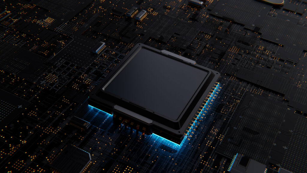
TSMC is inching closer to production for its new CoPoS (Chip-on-Panel-on-Substrate) advanced packaging. According to new reports, mass production of CoPoS is set to begin in the next six months.
The line represents the industry’s first large-scale attempt at panel-level packaging (PLP) for AI chips. That’s a meaningful shift. For years, the bottleneck for cutting-edge AI accelerators hasn’t only been the logic die itself — it’s been packaging, specifically TSMC’s CoWoS capacity. CoPoS is the company’s bet on what comes after, and Nvidia is reportedly first in line.
Technical breakthrough
The core change is geometry. TSMC’s current CoWoS (Chip-on-Wafer-on-Substrate) technology is built around 12-inch (300mm) circular silicon wafers. CoPoS swaps those round wafers for rectangular glass or organic panels measuring 310mm × 310mm — roughly 12.2 inches square. That sounds like a minor packaging detail, but the implications run deep.
The most immediate benefit is material utilization. Fitting square chip packages onto a round wafer wastes a lot of edge area, and CoWoS tops out at around 65% utilization. A rectangular panel pushes that much further, which cuts silicon waste and, by TSMC’s reckoning, trims per-unit costs by 20–30%. That’s a real number, not a rounding error, and it matters most at the scale these AI parts ship.
Size is the other half of the story. A larger panel means a larger usable package, and CoPoS is designed to support up to 12, and potentially more, HBM4 memory stacks alongside multiple GPU and CPU chiplets. Using glass or sapphire as the base layer rather than silicon also sidesteps the curvature problems that limit how big a silicon-based package can get, and TSMC is reportedly already eyeing even larger 515mm × 510mm panels for 2028–2029.
There’s a process angle too. CoPoS forms the silicon redistribution layers (RDL) on the panel first, then attaches the chiplets and HBM, then mounts everything onto an organic substrate. That ordering streamlines manufacturing compared to wafer-based methods. The headline, though, is simpler. More memory, less waste, bigger packages.
The Nvidia partnership
Nvidia has secured priority access to CoPoS, and it’s not hard to see why the company would want to lock that in early. The reported plan covers both its 2026 “Rubin” architecture and its 2028 “Feynman” AI platform, and it fits a pattern we’ve seen across the industry — the biggest players reserving packaging slots years ahead of need, because packaging capacity, not just wafer starts, has been the real constraint since 2024.
This also speaks directly to the memory wall, the long-standing gap between how fast accelerators can compute and how fast they can move data in and out of memory. More HBM stacks sitting closer to the logic doesn’t make the wall disappear, but it pushes it back, and it lays groundwork for the exascale AI systems being talked about for 2030.
The competitive read is straightforward. AMD and Broadcom both lean on the same TSMC packaging supply, and both remain tied to constrained CoWoS circular-wafer capacity. If Nvidia has priority access to a packaging technology that’s cheaper per unit and allows physically larger chips, that’s a structural advantage that’s hard to answer quickly. Add the cost angle — TSMC estimates CoPoS could shave a fair bit off AI chip production costs per unit at scale — and the appeal for cloud and data center buyers is obvious.
Realistic timelines?
The roadmap is aggressive. 2026 is about process refinement and yield testing with key partners, Nvidia chief among them. 2027 shifts to equipment expansion and scaling the pilot line toward final commercial validation. Mass production is expected to ramp in late 2028 through 2029 at TSMC’s Chiayi AP7 campus in Taiwan, in its P4 and P5 zones, with industry consensus pointing to the first commercial CoPoS chips shipping in late 2028.
The supply chain is moving to match. ASE Group, Amkor, and equipment vendors like Screen Semiconductor are scaling PLP-capable tools to TSMC’s 310mm panel standard, which over time means stepping away from the 300mm wafer infrastructure the whole industry has been built around. That kind of coordinated tooling shift is a decent signal that this isn’t a one-company science project. TSMC’s Arizona facility is also slated for phased CoPoS adoption after 2028, which conveniently addresses CHIPS Act pressure for onshore advanced packaging capacity.
That said, there are real reasons to hedge. The R&D bill for the pilot lines is estimated above $5 billion, and costs like that have a way of showing up in pricing — which would squeeze margins for fabless clients even as the per-unit packaging cost falls. Glass panels have also shown fragility in early testing, raising reliability questions that haven’t been fully answered yet.
Yield is the big one. Panels need new defect-control methods, and per Morgan Stanley’s analysis, failing to clear an 85% yield threshold by 2027 could push mass production back. That’s the kind of risk that doesn’t show up in a press release but determines whether the 2028 target holds.
CoPoS is an AI technology first and foremost — it offers only marginal gains for non-AI chips. So while it likely extends TSMC’s already dominant position in AI packaging, it doesn’t meaningfully broaden the company’s overall foundry lead. For AI accelerators, though, it could be the difference between hitting a packaging ceiling in 2028 and comfortably building past it.