Table of Contents
For decades, progress in silicon chips followed a consistent pattern: shrink transistors and pack more onto a die, which in turn, results in more powerful and more efficient chips. But that approach won’t last forever, thanks to escalating lithography costs and yield issues, which have resulted in transistor innovations no longer predictably declining in cost.
As a result, the industry is shifting focus. Instead of only scaling down transistors, designers are learning to scale up systems – by linking and stacking multiple chips to move data faster and more efficiently. We’re entering the era of advanced packaging, where the way transistors are connected may matter more than how small they are.
Here’s a look at the different approaches to semiconductor packaging, and what it could mean for the AI semiconductor industry in general.
2D integration

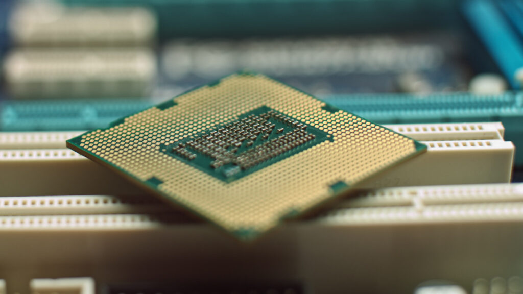
For most of the integrated circuit era, a chip meant a single, flat piece of silicon, known as a die, containing all of a device’s logic and memory. Each die is made up of tiny transistors, the microscopic switches that process digital signals. Over decades, engineers simply kept shrinking these transistors to fit more onto a single die, from a few thousand in the 1970s to tens of billions today. This 2D approach, where every circuit sits on one flat plane, made chips faster, cheaper, and more efficient for nearly fifty years.
Modern system-on-chip (SoC) designs integrate many blocks, including CPU cores, GPUs, memory caches, and I/O circuits, on that same slice of silicon. This “everything on one die” model remains efficient for most electronics, from smartphones to laptops.
Where 2D is used in AI
Even as packaging technologies advance, 2D integration remains the workhorse for most AI processing, and consumer electronics as a whole, today. These include the following.
- Consumer devices: Qualcomm’s Snapdragon X Elite and many other laptop chips combine CPU, GPU, and neural cores on one die.
- Edge and embedded AI: Compact processors like NVIDIA Jetson, Google Coral, and Hailo-8 use 2D SoCs for low-power inference near sensors.
- Mainstream GPUs: Products like NVIDIA’s GeForce RTX 40-series and AMD’s Radeon RX 7000 (except the high-end models) rely on traditional 2D layouts with external GDDR memory.
2D roadblocks
Despite its success, 2D scaling is running out of room to grow. Here are some roadblocks to 2D designs.
- Yield and cost: Larger dies with increasingly small transistors are harder to manufacture without defects, reducing yield and raising cost.
- Reticle limit: Lithography tools cap the maximum printable die size.
- Interconnect challenges: Shrinking wires increases resistance and power consumption, slowing data movement across the chip.
- Thermal density: Flat designs concentrate heat, limiting performance and efficiency.
While innovations like chiplets, which are smaller dies connected within one package, have helped improve yield and design flexibility, they can’t fully solve the physical limits of flat silicon. In short, 2D scaling has started to reach a point of diminishing returns.
2.5D integration

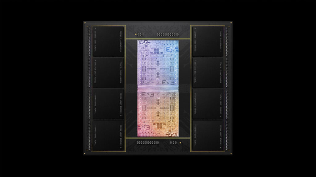
As chips reached the practical limits of what could fit on a single die, designers began looking for ways to combine multiple pieces of silicon inside one package. The result is 2.5D integration, where several dies sit side by side on a thin layer of silicon known as an interposer. The interposer acts like a high-speed highway between components, routing thousands of fine-pitch connections far more densely than a conventional package substrate.
A key innovation was the ability to place High Bandwidth Memory (HBM) directly beside the processor. By surrounding a GPU or accelerator die with stacked HBM modules on the same interposer, data can move over extremely short distances — enabling terabytes per second of bandwidth at far lower power. This architecture is ideal for AI and high-performance computing, where performance depends as much on data movement as raw compute power.
Where 2.5D is used in AI
2.5D packaging now underpins nearly all cutting-edge AI hardware, especially in settings like data centers. These include the following.
- NVIDIA H100 / H200: Built with TSMC’s CoWoS packaging, connecting a massive GPU die to multiple HBM3 or HBM3e memory stacks.
- AMD MI300: Integrates CPU, GPU, and HBM memory on a single interposer to create a unified compute-and-memory platform.
- Intel Ponte Vecchio (Xe-HPC): Uses EMIB silicon bridges to connect more than 40 chiplets across different process nodes.
- Custom AI accelerators: Startups like Tenstorrent, SambaNova, and Cerebras use 2.5D-style packaging to bring compute and memory closer together for large AI models.
2.5D roadblocks
While 2.5D integration has become the gold standard for AI accelerators, it brings new technical and economic limits of its own.
- Manufacturing cost: Silicon interposers add significant expense and require complex wafer bonding and alignment steps.
- Thermal management: Large, tightly packed dies generate heat unevenly, making cooling a major design challenge.
- Packaging capacity: Foundries like TSMC and Intel have limited production capacity for CoWoS and EMIB packaging, creating supply bottlenecks.
- Scaling limits: Even with interposers, dies still communicate horizontally, leaving some latency and power overhead compared to true 3D stacking.
While 2.5D solved many of the bandwidth and yield problems that constrained 2D design, it didn’t fully erase the physical distance between compute and memory.
3D integration

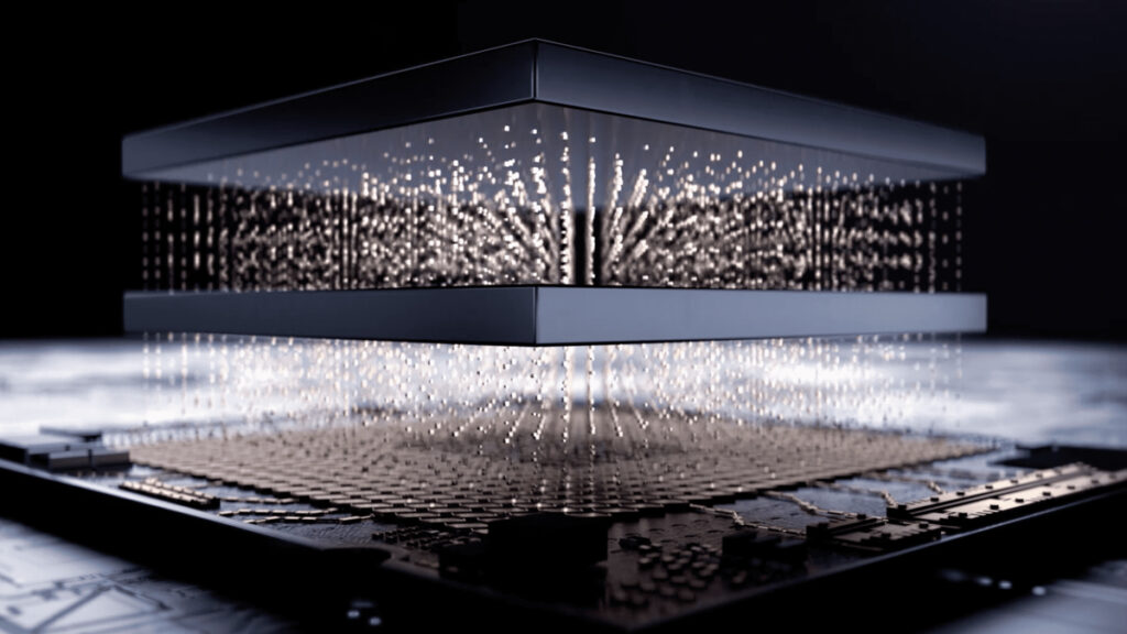
2.5D integration places chips side by side, but 3D integration takes the next leap by stacking them vertically. Instead of sending signals across a flat surface, engineers connect layers of silicon directly through the die, allowing data and power to move straight up and down. This adds a true third dimension to chip design, dramatically shrinking communication distances and enabling much higher density in the same footprint.
The key technologies are Through-Silicon Vias (TSVs), or microscopic holes filled with metal that carry data and power between stacked layers, and hybrid bonding, which connects dies face-to-face at extremely fine pitches. TSVs first appeared in High Bandwidth Memory (HBM), where multiple DRAM layers operate as a single ultra-fast unit. Hybrid bonding extends that concept to logic-on-logic stacking, achieving near on-die bandwidth. Together, these methods power platforms such as Intel Foveros, TSMC SoIC, and Samsung X-Cube, allowing multiple dies to behave almost like one chip.
Where 3D is used in AI
3D integration is quickly moving from experimental to commercial use, especially in AI and high-performance computing.
- AMD Ryzen 7 5800X3D / EPYC “Milan-X”: Use 3D V-Cache to stack additional cache directly on top of the CPU die for higher bandwidth.
- Intel Meteor Lake / Foveros Technology: Vertically stacks compute and I/O tiles, combining logic layers from different process nodes.
- TSMC SoIC-on-CoWoS: Used in AMD MI300 to combine 3D logic stacking with 2.5D interposers and HBM memory.
- Samsung X-Cube: Stacks logic and memory dies to reduce latency and improve energy efficiency for AI workloads.
3D roadblocks
3D stacking delivers powerful benefits, like greater density, faster data transfer, and lower energy per bit. But, it also introduces new physical challenges, like the following.
- Thermal management: Heat from upper layers must pass through multiple dies, making it difficult to cool hot logic blocks.
- Yield and reliability: One defective die can compromise an entire stack, raising costs and complicating testing.
- Manufacturing complexity: Aligning and bonding dies at micrometer precision demands new tools and processes.
- Design and testing overhead: 3D layouts require new co-design approaches that account for power delivery, thermals, and vertical interconnect timing.
By collapsing the distance between compute and memory, 3D integration achieves performance gains that traditional “flat” scaling cannot. But its cost and complexity mean it’s still limited to leading-edge processors.
Where packaging is headed
Chip design has evolved through several stages of integration, but that doesn’t mean that what you might consider to be traditional designs are going anywhere anytime soon. Most everyday processors in household devices still rely on 2D designs, where all components sit on a single flat die. However, at the high end, companies have started using 2.5D packaging, especially in advanced AI products and high-end GPUs.
3D integration is now starting to enter increased production though, as seen in AMD’s 3D V-Cache and Intel’s Foveros chips. And, as that production begins, ideas around the next stage have started forming. Here’s a look at future technologies in development:
- Chiplets and UCIe: Modular chiplets already sometimes replace large monolithic dies, each optimized for a specific role (compute, memory, I/O). The UCIe (Universal Chiplet Interconnect Express) standard aims to let these chiplets interoperate, even across vendors.
- System-on-Package (SoP): The natural successor to the SoC, SoP designs integrate compute, memory, power delivery, and networking directly into one package.
- Co-Packaged Optics (CPO): Optical interconnects will move onto the package, replacing long copper traces and cutting energy use for chip-to-chip communication.
- Glass and Fan-Out Substrates: New substrate materials and fan-out packaging enable finer wiring, larger packages, and better mechanical stability.
- Thermal and Power Co-Design: As integration increases, cooling and power delivery will become part of the package itself, using microfluidic channels, built-in regulators, and intelligent thermal management.
In short, 2D isn’t going away. It remains the foundation for most chips made today. But at the cutting edge of AI and high-performance computing, innovation now happens in how dies are connected, not just how small their transistors are. Yes, transistor innovations will continue, and they’ll still be important. But, the future of scaling arguably in the architecture of the entire package.


