
Table of Contents
The prototype shows how vertically stacked logic and memory could unlock major AI performance gains
In sum – what we know:
- A new kind of chip – Stanford researchers and SkyWater Technology successfully built the first monolithic 3D integrated circuit in a commercially active U.S. foundry, moving the technology out of academic labs.
- A big performance boost – The prototype stacks memory and logic layers vertically with high-density interconnects, achieving a 4x improvement in throughput and up to 12x gains in AI workload simulations.
- Big implications for AI – The project proves that cutting-edge 3D chip architectures can be manufactured domestically, addressing Moore’s Law limits and energy efficiency needs for data centers.
A collaboration between Stanford, Carnegie Mellon, University of Pennsylvania, and MIT has produced what the team calls the first monolithic 3D integrated circuit built at a commercial U.S. foundry.
That distinction matters: previous experimental 3D chips never left university cleanrooms. By working with SkyWater Technology, a domestic semiconductor manufacturer, the researchers showed that vertical chip architectures can actually be fabricated in a real production environment. The results were presented at the IEEE International Electron Devices Meeting (IEDM 2025) in December, and if the approach scales, it could dramatically change how AI processing hardware gets designed and built.
The tech specs
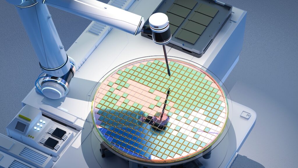
Instead of laying out circuits across a flat, two-dimensional plane, the prototype stacks memory and logic layers vertically — one on top of the other. The researchers compare it to floors in a skyscraper, with vertical wiring acting as high-speed elevators that shuttle data between levels. Crucially, this isn’t the same as current advanced packaging techniques that bond multiple finished dies together. Here, each layer is fabricated sequentially on the same wafer in one continuous process.
The chip combines several distinct technologies: standard silicon CMOS logic for compute, Resistive RAM for memory storage, and Carbon Nanotube Field-Effect Transistors (CNFETs). According to the researchers, the vertical interconnects represent the densest 3D wiring reported to date, dramatically shrinking the distance data has to travel between memory and processing units.
Thermal management posed one of the biggest engineering hurdles. Building multiple layers on a single wafer risks destroying previously fabricated circuitry during later manufacturing steps. The team solved this by designing the entire process around a low-temperature thermal budget of roughly 415°C, which protects underlying layers while still enabling sequential fabrication. SkyWater manufactured the chip on its 200mm production line using a mature 90nm to 130nm process — not the leading-edge nodes found at TSMC or Samsung, but sufficient to prove the architecture works.
Real performance gains
Hardware testing showed roughly a four-fold improvement in throughput compared with equivalent 2D implementations at similar latency and footprint. That’s a substantial gain, though with the obvious caveat that prototype results don’t always translate directly to production performance.
The simulation results were more impressive. When researchers modeled taller stacks with additional memory and compute tiers, they saw up to 12x performance improvements on AI workloads. These simulations drew on models based on Meta’s LLaMA architecture, suggesting the 3D approach could be particularly effective for large language models. The team projects that continued vertical scaling might eventually deliver 100x to 1,000x improvements in energy-delay product — a combined metric capturing both speed and efficiency. Those projections warrant healthy skepticism until validated in actual hardware, but they point to the ceiling the researchers believe the architecture can reach.
Big implications
Successfully fabricating this chip validates that U.S. foundries can produce advanced 3D architectures—a strategically significant point given ongoing concerns about semiconductor supply chains and national security. Mark Nelson, SkyWater’s Vice President of Technology Development Operations, called the project “an enormous challenge” to translate cutting-edge academic concepts into something a commercial fab could actually build.
For AI hardware, the results suggest 3D architecture could prove especially effective for large language models and data center workloads where energy efficiency matters most. As AI models continue growing in size and computational intensity, the energy costs of running them have become a major concern. Shorter data paths and tighter memory-compute integration could help address that bottleneck.
The work also offers an alternative path for continued performance scaling that doesn’t depend entirely on transistor miniaturization. Traditional Moore’s Law scaling—shrinking transistors to fit more on a chip—has grown increasingly difficult and expensive. Vertical integration opens a different dimension for improvement, though it brings its own manufacturing challenges.
SkyWater continues expanding its capacity through initiatives like its recent acquisition of Infineon Technologies’ 200mm fab in Austin, Texas, which added roughly 400,000 wafer starts per year. The company has also secured IP licensing agreements that could support broader adoption. Whether the 3D architecture demonstrated here moves from prototype to commercial production remains an open question, but the collaboration has at least established that the manufacturing pathway exists.