
Table of Contents
Cadence launches agentic ai system for end-to-end chip design
The new Cadence architecture automates the entire workflow from analog circuits to 3D-IC signoff
In sum – what we know:
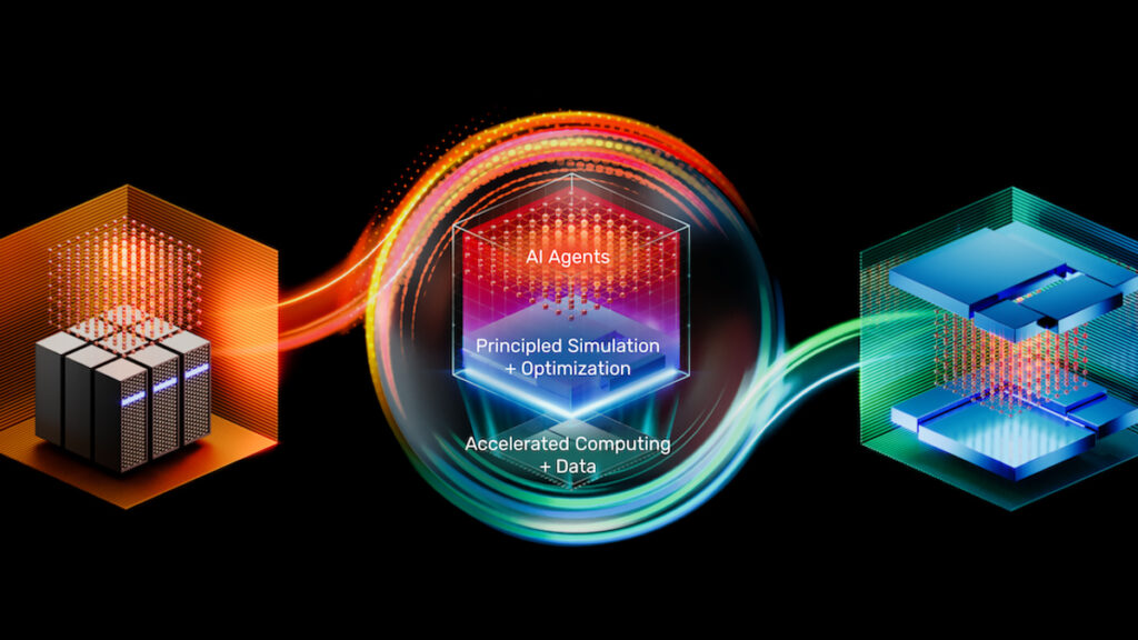
- Hierarchical agent architecture – The system uses a top-level orchestrator called AgentStack to coordinate three specialized agents—ChipStack, ViraStack, and InnoStack—covering the full design stack.
- Expansion into analog and digital – While ChipStack handles front-end verification, the new ViraStack automates difficult analog circuit migration, and InnoStack manages digital placement, routing, and signoff.
- GPU-accelerated 3D IC support – To address the extreme complexity of multi-die stacks, Cadence is leveraging its Millennium GPU platform for thermal, power, and voltage integrity analysis in 3D designs.
Cadence Design Systems has announced what is arguably its most ambitious agentic AI product launch yet — a system build to design new chips end-to-end, including new 3D-IC designs. The system is built on a hierarchical agent architecture, with a top-level orchestrator called AgentStack coordinating three domain-specific AI Super Agents that collectively span the full chip design stack.
CEO Anirudh Devgan positioned the launch as a deliberate push to extend agentic AI well beyond the front-end RTL and verification work where it’s already proven useful. The ambition is to cover the entire chip design workflow, from analog circuit design all the way through digital back-end signoff. Whether the platform actually delivers on that promise at scale is, of course, a question only production silicon can settle.
The three AI super agents
Each of the three super agents owns a distinct chunk of the chip design workflow, with specialized capabilities tailored to its domain. ChipStack, which launched earlier, covers front-end design and verification. It’s the backbone of Cadence’s broader Mental Model architecture and has posted productivity improvements of up to 10X. Being the most mature of the three, ChipStack essentially sets the blueprint for how ViraStack and InnoStack are expected to develop over time.
ViraStack made its debut at CadenceLIVE 2026, targeting custom analog circuit design and migration — an area that has stubbornly resisted automation because it depends so heavily on seasoned analog engineers navigating subtle design tradeoffs. Early customers are reportedly citing 3–10X productivity gains, which, if they hold up across broader deployments, would mark a real inflection point in how analog teams work. The fact that agentic AI is making inroads in analog at all is significant — it’s a fundamentally harder problem than digital automation. That said, the wide spread of that 3–10X range hints that results depend a lot on the specific workflow.
InnoStack, also new at the event, handles the digital back-end, including placement, routing, and signoff closure. With InnoStack now in play, Cadence claims full coverage of the monolithic chip design flow across its three super agents.
AgentStack orchestration
AgentStack operates above the three domain-specific super agents as a unified orchestration layer, coordinating work across all of them. The core idea is to abstract away much of the complexity engineers currently wrangle by hand, letting them work at a higher conceptual level instead of slogging through task-level details. In theory, an engineer could express design intent and let the orchestrator sort out which agents need to fire, in what sequence, and how their outputs chain together.
What makes this architecture interesting is how Cadence constrains what the agents can actually do. Instead of letting LLM-generated suggestions run wild, the Mental Model architecture anchors agent behavior within established EDA tool parameters. Simulation, optimization, bespoke neural networks, and LLM reasoning all work together without changing how the underlying solver engines operate.
The early numbers from ChipStack look promising — Cadence reported high bug injection catch rates and formal verification timelines shrinking from days to hours. In a domain where verification bottlenecks routinely eat project schedules alive, those are meaningful results. Still, Cadence itself is upfront that the real proof will come from production silicon, not demos and benchmarks. The industry has seen enough gap between controlled results and production reality to know the difference.
The 3D IC challenge
For all the momentum on monolithic chip design, Cadence’s CEO flagged 3D IC signoff as a major bottleneck. Signoff complexity explodes when you move into high-layer-count stacks like 12–16 layer HBM configurations and multi-chiplet packages. These designs bring compounding challenges that simply don’t exist in traditional 2D flows, like thermal gradients shifting across die layers, voltage integrity issues spanning multiple chips, die-to-die interface verification, and cross-die signoff requirements that multiply with every additional chiplet.
For now, rather than waiting on a purely agentic solution, Cadence is extending its Millennium GPU-accelerated platform to tackle 3D IC workloads. Millennium, previously deployed for circuit simulation through Spectre and CFD via Cascade, is being pointed at 3D IC-specific problems, like voltage IR drop analysis, power integrity simulation, thermal analysis across multi-chiplet packages, and multi-chiplet stress simulation. Allegro X AI serves as a complementary piece within this GPU acceleration strategy.
Strategic partnerships and business model evolution
Cadence isn’t trying to build this ecosystem in isolation. An expanded collaboration with NVIDIA, building on an earlier GTC 2026 announcement, pairs Cadence’s agentic EDA tools with NVIDIA’s CUDA-X libraries, AI physics simulations, and Omniverse platform. The aim is to accelerate GPU-native chip and system design, which makes obvious strategic sense given how much of the Millennium platform’s value is tied to GPU compute. A parallel partnership with Google Cloud integrates ChipStack with Google’s Gemini foundation models, giving Cadence access to frontier LLM capabilities without having to develop everything internally.
On the business model side, there’s a notable pivot toward consumption-based pricing alongside traditional license structures. The new approach ties value to the scale of design work completed — essentially measuring the output delivered by “virtual engineers” working alongside human teams. That’s a meaningful departure from how EDA software has historically been sold, and it aligns Cadence’s revenue more directly with the productivity improvements it’s promising. Whether customers actually go for it will come down to consistency. If results are uneven, it starts to feel more like a liability.
Next-gen chips
The idea behind the system isn’t surprising. The goal is to automate the repetitive tasks, lower barriers for newcomers, and address the chronic shortage of chip design talent. These goals have been around for a long time, and agentic AI represents the latest technology aimed at actually achieving them. Cadence is also positioning its expanded capabilities to serve physical AI applications like autonomous vehicles, robotics, and drones, where chip complexity and design iteration speed matter more than ever.
Turns out, industry standardization plays a bigger role here than it might seem at first glance. Standards like UCIe (Universal Chiplet Interconnect Express) are going to be essential for interoperability across the complex multi-chip packages that 3D IC designs require. Without broad adoption, even the most capable AI agents will run headlong into the fragmentation baked into multi-vendor chiplet ecosystems.