

Table of Contents
HBM4E triples bandwidth per stack, but volume production waits for 2027
In sum – what we know:
- Same interface, more speed – HBM4E keeps HBM4’s 2,048-bit width and pushes per-pin rates to 14 to 16Gbps for about 3.6TB/s per stack.
- No standard yet – As of October 2026 the published specs cover HBM4 and SPHBM4, leaving HBM4E a vendor-defined generation with no independent benchmarks.
- Sold out before it ships – Samsung says 2026 HBM4 volume is effectively sold out, and Micron has much of its 2027 supply locked in at higher prices.
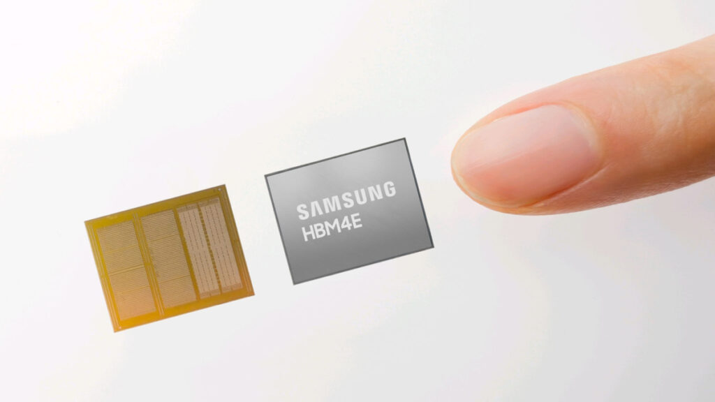
Samsung and SK hynix have both shipped 12-high HBM4E samples to major customers, in what Samsung calls the first silicon of the seventh generation of high-bandwidth memory (HBM). Samsung’s shipment arrived in late May, with SK hynix following a few weeks later. Neither company has announced a mass production date. Micron, the third major HBM supplier, expects its own HBM4E volume production in calendar 2027.
HBM has become the most critical and supply-constrained component in AI infrastructure. Many major AI accelerators depend on it, from Nvidia’s Blackwell and Rubin platforms, to AMD’s Instinct series and Google’s TPUs, and this next generation is arriving into a market where current supply is already severely allocated. Samsung reported that HBM4 volume for 2026 is effectively sold out, and SK hynix said its full 2026 DRAM and NAND output is sold out. A new memory generation is being fought over before volume production even begins.
What is HBM4E?
HBM4E is the successor to HBM4, a form of stacked DRAM designed to feed the bandwidth demands of AI accelerators. HBM4 is already in high-volume production — Samsung began shipping it in February and Micron in March — making HBM4E the next step in a roadmap that’s moving unusually fast. The generation keeps HBM4’s wider 2,048-bit interface while pushing per-pin data rates significantly higher, yielding more bandwidth, more capacity, and better power efficiency per stack.
Samsung shipped 12-high HBM4E samples in late May. SK hynix followed roughly three weeks later. Samsung frames HBM4E as targeting large language models and next-generation AI systems, while SK hynix positions it for AI training, inference, and large-scale datacenter deployments.
How HBM4E differs from earlier HBM generations
HBM3E
HBM3E, the generation powering systems like Nvidia’s Blackwell-based GB200, uses a 1,024-bit interface rated at roughly 9.2 to 9.6Gbps per pin, though shipping accelerators ran slower and higher-rated parts have been announced. That delivers about 1.2TB/s of bandwidth per stack, with a typical 12-high stack holding 36GB. It’s fast memory, and it’s what most of the AI industry runs on.
HBM4E is a generational leap from that baseline. The interface doubles to a 2,048-bit width, a change that actuallyoriginated with HBM4, and per-pin data rates climb to 14 to 16Gbps. The combined effect is roughly triple the per-stack bandwidth of HBM3E, along with a bump to 48GB per 12-high stack. The biggest architectural shift, the doubling of interface width, happened with HBM4. HBM4E builds on that foundation with speed and efficiency gains.
HBM4
The HBM4-to-HBM4E transition is more incremental. Interface width stays at 2,048-bit. The main change is speed. JEDEC’s HBM4 spec publishes a top speed of 8Gbps per pin, though vendors have been shipping faster in practice — Samsung measured its HBM4 at 11.7Gbps in system-in-package testing. HBM4E pushes that to 14 to 16Gbps, about 20% over Samsung’s measured speed at the low bin and roughly 37% at 16Gbps.
Samsung’s headline figure is about 3.6TB/s per stack, with 4.1TB/s reflecting an extrapolation to 16Gbps; the comparison point is roughly 2.0TB/s for HBM4 at the JEDEC rated 8Gbps. Claims that HBM4E “doubles HBM4 bandwidth” hold only against that rated figure, not against the 11.7Gbps vendors are actually delivering. Power and thermal improvements in this generation come primarily from DRAM process refinements, base-die changes and packaging, not from fundamental architectural rework.
Architecture and what changes
HBM4E carries over the 2,048-bit interface from HBM4, organized into 32 channels per stack with two pseudo-channels per channel. The interface width hasn’t changed, but the speed increase has system-level consequences. Six HBM4E stacks on a single accelerator, a common configuration for high-end AI chips, would deliver roughly 24.6TB/s of aggregate bandwidth according to Rambus calculations. That compares to about 12.3TB/s from six HBM4 stacks at the JEDEC baseline.
Power efficiency gets attention too. The data bus voltage (VDDQ) can drop to the 0.7 to 0.9V range, which reduces energy per bit transferred. Samsung claims 16% better energy efficiency and more than 14% lower thermal resistance versus its prior generation, while SK hynix reports more than 20% better power efficiency and 17% improved heat resistance over HBM4. These are vendor numbers — no independent benchmarks of HBM4E silicon have been published.
Backward compatibility with HBM3 memory controllers should ease adoption for accelerator designers already working with existing HBM platforms. The generation adds Directed Refresh Management to help mitigate row-hammer vulnerabilities, a growing concern as DRAM cells shrink and become more susceptible to interference from neighboring reads. Rambus has announced HBM4E controller IP rated for 16Gbps per pin, though that remains a vendor product announcement rather than shipping silicon.
Sample status and timing
Samsung says mass production timing will be “aligned with customer schedules,” after initial sample shipments and optimization, without naming a date. SK hynix has been similarly noncommittal, stating it “will work closely with partners for mass production in a timely manner,” but has publicly targeted 2027. Micron points to 2027 as well.
The distance between sampling and volume shipping is significant. KED Global reported in early October that Samsung’s 12-high HBM4E passed qualification testing with Nvidia and major hyperscalers, though neither Samsung nor Nvidia has officially confirmed that. If accurate, it would be a meaningful win for Samsung — its HBM3E reportedly failed early qualification attempts and its eventual clearance was disputed before it was later reported qualified, while Nvidia has confirmed all three vendors for HBM4. SK hynix, by contrast, has remained Nvidia’s primary HBM supplier and reportedly has long-term agreements with around 10 major customers.
There are broader questions around standardization, too. No JEDEC HBM4E standard has been confirmed as of October 2026 — the published standards are JESD270-4A, covering HBM4, and JESD330-4, covering SPHBM4. That makes HBM4E a vendor-defined product generation for now, rather than a unified industry specification. Samsung, SK hynix, and Micron can ship meaningfully different implementations under the same label, and no independent benchmark exists to verify any of the performance claims being made.
Role in AI workloads
Modern AI workloads are increasingly bandwidth-bound. When an accelerator stalls waiting for data, it isn’t computing — and those memory stalls are one of the main reasons raw FLOPS numbers don’t translate cleanly into real-world throughput. HBM delivers far more bandwidth per package than any other memory type, which is why every major AI accelerator from Nvidia’s H100 onward has depended on it.
Capacity has scaled rapidly alongside bandwidth. The H100 shipped with 80GB of HBM3. Nvidia’s Blackwell-based accelerators pair with up to 192GB of HBM3E, and the GB200 NVL72 rack pools up to 13.5TB across its GPUs. AMD’s upcoming MI450 targets 432GB of HBM4 per accelerator. Fitting larger models within a single node reduces the cross-node communication overhead that eats into training and inference efficiency.
Samsung markets HBM4E as essential for “LLMs and next-generation AI systems.” SK hynix positions it for “AI training and inference” and “large-scale computing systems.” Those are vendor positioning statements, but the underlying need is real. For inference workloads, particularly autoregressive decoding where the model generates output one token at a time, throughput often tracks closer to memory bandwidth than to peak compute. More bandwidth per stack should mean faster token generation, larger key-value caches for maintaining session context, and more concurrent users per accelerator. In practice, though, stack-level bandwidth improvements don’t map directly to proportional performance gains. Batching, parallelism, software optimization, model architecture, and cooling all factor in. A doubling of stack bandwidth doesn’t mean a doubling of inference speed.
The memory shortage
All of this is playing out against what is the tightest memory market in years. Samsung said on its Q1 2026 earnings call that HBM4 volume for 2026 is effectively sold out. SK hynix has said its 2026 DRAM and NAND output is fully sold out. Micron says much of its 2027 supply is already locked in at higher prices, with many sales discussions now focused on 2028.
The underlying problem is structural. HBM uses roughly three times the wafer capacity of DDR5 per gigabyte, meaning every wafer dedicated to HBM production is one that can’t supply PCs, phones, or conventional servers. As AI demand pulls more fab capacity toward HBM, conventional DRAM supply tightens. Q1 2026 conventional DRAM contract prices rose about 93 to 98% quarter over quarter, according to TrendForce. The consumer impact is tangible — PC makers have flagged system prices rising 15 to 20% on the back of memory costs, and one tracked retail 32GB DDR5-6000 kit was listed at $402 in August 2026, where the same kit sold for roughly $110 to $140 a year earlier.
HBM pricing has grown even more extreme. A 36GB HBM3E module was trading at approximately $2,100 on the spot market as of early September 2026, roughly four to five times long-term contract prices. Korean export data shows the average unit price across the broader memory export category rose roughly 37% between May and July 2026, with HBM-specific figures up roughly 31% over the same stretch. TrendForce projected blended HBM ASPs up roughly 121% in a September 2026 forecast, while UBS projects average selling prices up about 79%. Those are analyst forecasts, not realized prices, but they all point in one direction.
Capacity relief is slow in coming. SK hynix broke ground on an advanced HBM packaging and test facility in Indiana in August 2026, but that site won’t have a cleanroom until October 2028, with HBM4E volume production targeted for the second half of 2029. Its Yongin cluster in South Korea targets a Y1 cleanroom in February 2027, with June 2029 now the target for Y2. New fabs take years to bring online.
From a supply standpoint, HBM4E adds little relief before 2027 at the earliest. It requires more DRAM dies per stack than shorter configurations, advanced logic base dies fabricated at leading-edge process nodes, and fresh qualification cycles before volume shipments can begin. No public source has quantified HBM4E’s direct effect on the broader shortage, but more demand stacked on top of already-constrained supply doesn’t ease anything. If anything, it intensifies the pressure that’s already reshaping memory economics across the industry.