

Table of Contents
Maia 300 bets on tokens per watt, not peak compute
In sum – what we know:
- Memory-first design – Maia 300 packs 288GB of HBM4 at 18 TB/s across a chiplet layout, matching Nvidia’s Blackwell Ultra while trailing AMD’s 432GB MI455X.
- A 2027 ramp – Production starts next year with a claimed 40% gain in tokens per megawatt, though Maia 200 only recently expanded beyond two US data centers.
- No outside customers – There’s no public Azure SKU for Maia, so the chip serves only Microsoft’s own workloads while Google and Amazon rent their custom silicon to anyone.
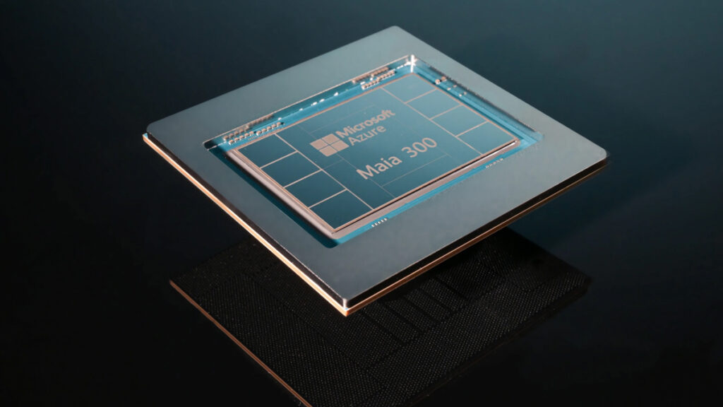
Microsoft has unveiled the Azure Maia 300, the third generation of its custom AI accelerator, at the OCP Global Summit in San Jose. The chip won’t enter production until 2027, but Microsoft is already laying out plans for “multi-gigawatt deployments” once it does. According to EVP Scott Guthrie, Maia should become “the primary inference system for Microsoft products and services.” CEO Satya Nadella called it “our biggest bet yet on our own silicon.” Reuters reports the company plans to deploy potentially more than one million units next year.
The scale of that commitment is significant, but the framing around it matters more. Rather than leading with peak compute, Microsoft built its pitch around tokens per watt and data movement efficiency. Inference is a recurring cost that compounds across every Microsoft product, from Copilot to Teams to Azure. Making it cheaper per token matters more, in dollar terms, than making any single request faster.
That said, Maia 200, the current generation, was reportedly running in only two US data centers as of August, according to The Information. Scaling a custom chip program across a global cloud footprint is a fundamentally different challenge than designing the silicon. Microsoft is betting that owning the chip beneath its inference workloads will compound savings across billions of daily requests.
Chip and rack specifications
Maia 300 uses a multi-chiplet design. Compute chiplets are fabbed on TSMC’s N2P node, a 2nm-class process, while the memory-controller and I/O chiplets sit on 3nm. Each is built on the node best suited to its function. The chip draws up to 950W, up from Maia 200’s 750W, and delivers roughly 13.8 petaflops at four-bit precision (FP4) and 6.9 petaflops at eight-bit (FP8). Microsoft says that’s a 36% increase in system compute FLOPs over the previous generation.
Memory is where the bigger generational leap shows up. Maia 300 packs eight stacks of HBM4 (high-bandwidth memory) totaling 288GB, with 18 TB/s of peak bandwidth. Maia 200 shipped with 216GB of HBM3E at 7 TB/s, so the jump is 33% more capacity and 2.5 times the bandwidth. For broader context, Nvidia’s B200 uses 192GB of HBM3E per GPU, while its Blackwell Ultra (B300) ships with 288GB — the same as Maia 300 — and AMD’s MI455X, part of the now-shipping MI400 series, uses 432GB of HBM4. The memory layout also shifts from uniform access on a monolithic chip to a NUMA (non-uniform memory access) organization across chiplets, letting software place data closer to the compute that needs it. Microsoft has been consistent in framing data movement — not raw compute — as the primary bottleneck for large inference systems, and the memory redesign reflects that.
The underlying architecture builds on SDLA, the Software Defined Locally Accessed Dataflow Architecture Microsoft introduced with Maia 200. It separates the control path from the data path, with software explicitly managing on-die SRAM as locally accessed scratchpad memory to reduce pressure on HBM. Maia 300 adds hardware support for aggressive low-precision formats, including MXFP4 (a microscaling four-bit format) and sub-three-bit storage, with accelerated conversion between them. The aim is to cut bytes moved per token and shrink the KV-cache — the working memory that holds model context during active sessions — enabling larger context windows and more concurrent users within the same power envelope.
At the rack level, density doubled. Maia 300 fits 96 accelerators per rack in a 167 kW envelope, up from 48 for Maia 200. That’s 27.6 TB of HBM and 1.7 PB/s of aggregate bandwidth per rack. A full superpod scales to 12,288 accelerators across 128 racks, double the 6,144-accelerator ceiling of the previous generation.
Networking runs on Ethernet with a custom AI transport layer — a deliberate contrast to Nvidia’s proprietary NVLink interconnect. The topology is two-tiered, with direct links between accelerator pairs in a tray and switched fabric across all 96 accelerators in the rack, plus optical connections for cross-rack traffic. Each accelerator gets 3.2 TB/s of bidirectional scale-up bandwidth, and the split between in-rack and cross-rack bandwidth is a runtime parameter rather than a fixed design choice, so job packing can adjust it on the fly. Liquid cooling removes more than 80% of the thermal load, with air handling the rest for memory and storage.
Performance claims and rollout timeline
Microsoft says it expects Maia 300 to deliver 40% more tokens per megawatt than “leading GPU-based systems.” It also claims up to 7x rack-scale token throughput versus Maia 200 and more than 2.5x improvement in performance per watt over the previous generation. On paper, those are substantial gains.
Production deployments are scheduled for 2027, with more detail expected at Microsoft Ignite in November. Maia 200 currently serves workloads for Microsoft 365 Copilot and Microsoft’s MAI model development team. GitHub Copilot and Microsoft Foundry are expected to come online by end of 2026. But the deployment base has been narrow. The Information reported in August that Maia 200 was running in only two US data centers — not exactly the kind of footprint that inspires confidence in a multi-gigawatt ramp.
Analysts aren’t expecting a rapid transformation. Evercore ISI estimates Maia will account for roughly 10% of Microsoft’s AI chip spending by early 2027. Wedbush analyst Matt Bryson has noted that Microsoft has had a tough time scaling earlier Maia versions. Supply is the binding constraint on the Maia 300 ramp. Microsoft is reportedly negotiating for more than 300,000 units for 2027 delivery, and Maia GM Andrew Wall said the company is securing HBM supply roughly five years out — a stark shift from the one-to-two-year planning horizon the industry used to work with. Microsoft’s FY2026 capital expenditure hit $115.95 billion, up around 80% year over year, with management guiding to roughly $175 billion for calendar 2026. The multi-gigawatt Maia commitment is partly a payoff test on that spending.
Competition
Unlike the Maia 200 launch in January, which named specific rivals, the Maia 300 announcement avoids direct comparisons entirely. That’s probably wise given the claims are forward-looking and unmeasured, but it makes the pitch harder to evaluate.
The field for custom AI inference silicon has grown crowded. Google sells its TPUs directly to cloud customers. Amazon’s Trainium chips are available on AWS, with Anthropic reportedly committed to deals for around one million of them. OpenAI unveiled its Broadcom-built Jalapeño inference chip in June. Meta continues developing its MTIA accelerator. Each represents a different bet on how inference economics should work, and each chips away at Nvidia’s dominance from a different angle.
Maia occupies a distinct — and somewhat limiting — position among them. There’s no public Azure SKU for the chip, meaning outside customers can’t rent Maia-backed instances the way they can rent Google TPU or Amazon Trainium capacity. That confines Maia’s reach to Microsoft’s own products and services, at least for now. Microsoft hasn’t committed to a firm timetable for broader availability.
Microsoft also isn’t walking away from GPUs. Alistair Speirs, general manager of Microsoft’s global infrastructure, has said the company continues to partner with Nvidia and AMD for model training. On the July earnings call, Nadella said Microsoft will be among the first cloud providers to deploy Nvidia’s Vera Rubin and AMD’s Helios rackscale systems. Microsoft publicly committed in July to ramp AMD Helios on Azure — the first hyperscaler to do so — and Nadella shared a stage with Nvidia’s Jensen Huang as recently as last week to launch Windows PCs built on Nvidia chips.